

- - Le physicien français Alexandre-Edmond Becquerel (3/24/1820 - 5/11/1891) a observé l'effet photoélectrique en 1839, par l'intermédiaire d'une électrode dans une solution conductrice exposée à la lumière. En 1905, Albert Einstein a donné l'interprétation scientifique de l'effet photoélectrique (affaire de photon - prix Nobel de physique en 1921).
Cet effet exploite les attributs des matériaux de semi-conducteur tels que le silicium Si qui est largement disponible. Un semi-conducteur est un matériel plein dont la conductivité électrique se fait entre celle d'un conducteur et un isolateur.
Comme nous le savons, l'atome est la plus petite particule qui comporte un élément chimique. Un atome se compose de coquilles d'électron qui entourent un noyau dense. La coquille extérieure d'électron d'un atome dans son état non lié est connue comme coquille de valence, et les électrons dans cette coquille s'appellent les électrons de valence. Chaque atome tend à avoir 8 électrons dans sa coquille externe. L'atome de silicium dans sa coquille de valence contient 4 électrons qui forment un tétraèdre régulier, au centre est le noyau. Chaque atome de silicium, afin de compléter sa coquille de valence avec 8 électrons, collabore avec 4 autres atomes de silicium qui l'entourent, constituant des couples d'électron. Il prend ainsi la forme d une structure en cristal de silicium. Les électrons de valence d'un conducteur sont très agiles et en raison de cette agilité les attributs d'un matériel de conducteur existent. Au contraire, dans les isolateurs les électrons de valence sont puissamment reliés au noyau et en raison de cela les attributs du matériel de isolateur existent. Dans les semi-conducteurs, les électrons de valence
 sont reliés de manière relativement lâche au noyau, dont ils ont l'agilité; si l un des électrons du conducteur d une façon ou d'une autre obtient une énergie additionnelle de prises d'électron, il peut casser ses obligations avec le noyau et partir loin de ceci. L'endroit dont l'électron est parti est une région a déficit électronique et présente une charge positive égale a celle de l'électron et s'appelle le trou d'électron. L'énergie additionnelle que les électrons devraient prendre afin de partir de l'atome, peut être offerte par la chaleur ou l'éclairage. La lumière est constituée par les petites particules qui s'appellent les photons qui transportent l'énergie.
 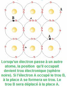 Quand la lumière heurte un semi-conducteur, certains des photons heurtent les électrons de valence et leur transmettent a tous leur énergie. Si, donc, la lumière heurte un cristal de silicium, dans son intérieur nous "verrons" quelques électrons abandonner les atomes correspondants et s'attacher a d'autres atomes. Dans le cristal du silicium il y a des atomes avec 9 électrons dans la coquille extérieure, ils sont négativement chargés, et l'atome avec 7 électrons dans la coquille extérieure ou différemment, avec un trou d'électron dans la coquille extérieure, celui-ci est positivement chargé. D'autres électrons sont également libérés et ils sont attachés en atomes qui occupent l'endroit d'un trou d'électron. En raison de ce processus, un mouvement irrégulier des électrons et des trous d'électron est créé, qui cependant n'est pas équivalent au courant électrique. Le courant électrique est un mouvement dirigé et concret des électrons ou des trous d'électron. Le mouvement dirigé des électrons et des trous d'électron est réalisé
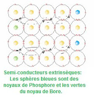 avec le semi-conducteur extrinsèque. Semi-conducteurs extrinsèques : Un semi-conducteur propre chimique ne peut pas fonctionner comme générateur photoélectrique, en raison du mouvement irrégulier des électrons et des trous d'électron dans la structure en cristal. Nous prenons un cristal de silicium et on l enduit de Phosphore (P) a droite et du Bore (B) sur son côté gauche. Les éléments de P et de B sont dans les électrons extérieurs de la coquille respectivement 5 et 3. Le pourcentage d'"enduit" s'élève en 1014 à 1017 atomes P ou B par cm3 de cristal de silicium. Avec "l enduis" en structure en cristal quelques atomes de silicium sont remplacés par des atomes de P et de B. Ainsi, quelques atomes de silicium ont dans des électrons de la coquille 9 de valence du côté qui "a été enduit" avec P et 7 électrons du côté que "a été enduit" avec B. En d'autres termes, du côté de P nous avons les électrons superflus en coquille de valence, alors que du côté de B nous avons des déficits électroniques dans la coquille de valence, ou trous d'électron. Cependant le cristal est neutre électriquement. Si la lumière heurte le cristal "enduit", du côté de P les électrons et étant libérés (et superflus), avec des sauts seront déplacés du côté de B, afin d'occuper les vides électroniques, ou les trous d'électron. De cette façon, nous réalisons l'accumulation de B des électrons, en d'autres termes des charges négatives et dans la région de l'accumulation de P des trous d'électron, ou de charge positive. Ainsi, entre les deux surfaces, la tendance électrique en cristal "enduite" sera créée. Le cristal "enduit" du silicium fonctionne comme source électrique avec le poteau positif du côté de P et le poteau négatif du côté de B. Connectant une lampe aux deux poteaux du cristal "enduit" du silicium, cette action sera accompagnée du mouvement des électrons, en d'autres termes du courant électrique.
~ Μitropoulos Αntonis – élève de 1eres, Lycée Léonin de Nea Smyrni. - - The photoelectric effect was observed in 1839 by the French physicist Alexandre-Edmond Becquerel (3/24/1820 – 5/11/1891), via an electrode in a conductive solution exposed to light. In 1905 the Albert Einstein (3/14/1879 - 5/18/1955) gave the scientific interpretation of photoelectric effect (affair of photon - Nobel Prize in physics of 1921).
This effect exploits the attributes of semiconductor materials such as silicon Si which is widely available. A semiconductor is a solid material that has electrical conductivity in between that of a conductor and that of an insulator.
As we know, the atom is the smallest particle that comprises a chemical element. An atom consists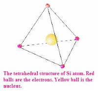 of electron shells that surround a dense nucleus. The outermost electron shell of an atom in its uncombined state is known as the valence shell, and the electrons in that shell are called valence electrons. Each atom tends to have 8 electrons in its outer shell. The atom of Si in its valence shell contains 4 electrons that are in the tops of one regular tetrahedron, in the centre of which is the nucleus. Each atom of Si, in order to supplement its valence shell with 8 electrons, collaborates with other 4 atoms of Si that surround it, contributing per couple from an electron. Thus takes shape the crystal structure of Si. The valence electrons of a conductor are very agile and because of this agility the attributes of a conductor material exist. On the contrary, in the insulators the valence electrons are very powerfully connected with the nucleus and because of that owed the attributes of the insulator material exist. In semiconductors the valence electrons are connected relatively relaxedly with the nucleus, without they have the agility
 of conductor’s electrons. If somehow, an electron takes additional energy, it can break its bonds with the nucleus and leave away from this. The place from which the electron left is a region with electronic deficit and presents positive charge equal with that of electron, it is called electron hole. The additional energy that electrons should take in order to leave from the atom, can be offered with heat or lighting. The light is constituted by small particles that are called photons and they transport energy. When light strikes a semiconductor, some of the photons collide with the valence electrons and transmit in them all of their energy.
 If, therefore, light strikes a crystal of Si, in its interior we shall “see” some electrons abandoning the corresponding atoms and attaching themselves in other atoms. In the crystal of Si there are atoms with 9 electrons in the outermost shell, that are negative charged, and atom with 7 electrons in outermost shell or differently, with an electron hole in outermost shell, that are positive charged. In meanwhile other electrons are also released and they are attached in atoms or occupy the place of an electron hole. As a result of this process an irregular movement of electrons and electron holes is created, which however is not equivalent to electric current. The electric current is a directed and concrete movement of electrons or electron holes. The directed movement of electrons and electron holes are achieved
 with the extrinsic semiconductor. Extrinsic semiconductors : A chemical clean semiconductor cannot function as a photoelectric generator, because of the irregular movement of electrons and electron holes in the crystal structure. We take a crystal of Si and “doping” it with Phosphor (P) from the right and with Boron (B) from its left side. The P and B elements have in outermost shell respectively 5 and 3 electrons. The percentage of "doping" amounts in 1014 to 1017 atoms P or B per cm3 of crystal of Si. With "doping" in crystal structure some atoms of Si are replaced by atoms of P and of B. Thus some atoms of Si have in valence shell 9 electrons from the side that "was doped" with P and 7 electrons from the side that "was doped" with B. In other words, from the side of P we have redundant electrons in valence shell, while from the side of B we have electronic deficits in valence shell, or electron holes.
 - - Το φωτοηλεκτρικό φαινόμενο παρατηρήθηκε το 1839 από τον Γάλλο Φυσικό Alexandre Edmond Becquerel, (24/3/1820 – 11/5/1891) ο οποίος ανακάλυψε ότι μπορεί να παραχθεί ηλεκτρικό ρεύμα όταν συγκεκριμέ- νες κατασκευές εκτεθούν στο φως. Το 1905 ο Albert Einstein (14/3/1879 - 18/5/1955) έδωσε την επιστημονική ερμηνεία του φωτοηλεκτρικού φαινόμενου (υπόθεση του φωτονίου – βραβείο Nobel φυσικής το 1921).
Το φαινόμενο αυτό εκμεταλλεύεται τις ιδιότητες των ημιαγώγιμων υλικών όπως είναι το πυρίτιο Si το οποίο βρίσκεται σε αφθονία στη φύση. Ημιαγωγοί ονομάζονται τα σώματα εκείνα που σε κατάλληλες συνθήκες μπορούν να λειτουργήσουν είτε ως αγωγοί είτε ως μονωτές.
Όπως γνωρίζουμε, η ύλη αποτελείται από άτομα. Κάθε άτομο, με τη σειρά του, αποτελε ίται από τον πυρήνα και από τα ηλεκτρόνια που περιστρέφονται γύρω απ’ αυτόν, τοποθετημένα πάνω σε στοιβάδες. Από τα ηλεκτρόνια τα πιο απομακρυσμένα από τον πυρήνα, αυτά της εξωτερικής στοιβάδας, λέγονται ηλεκτρόνια σθένους και η αντίστοιχη στοιβάδα, στοιβάδα σθένους. Κάθε άτομο επιδιώκει να συμπληρώσει την εξωτερική του στοιβάδα με 8 ηλεκτρόνια. Το άτομο του Si στην στοιβάδα σθένους περιέχει 4 ηλεκτρόνια, που βρίσκονται στις κορυφές ενός κανονικού τετράεδρου, στο κέντρο του οποίου βρίσκεται ο πυρήνας. Για να συμπληρώσει τη στοιβάδα σθένους του με 8 ηλεκτρόνια, κάθε άτομο Si συνεργάζεται με άλλα 4 άτομα, που το περιβάλλουν στο χώρο και συνεισφέρουν ανά δύο από ένα ηλεκτρόνιο. Έτσι σχηματίζεται το κρυσταλλικό πλέγμα του Si. Στους αγωγούς του ηλεκτρισμού τα ηλεκτρόνια σθένους είναι πολύ ευκίνητα και σ΄ αυτήν την ευκινησία οφείλονται οι αγώγιμες ιδιότητες του υλικού. Αντίθετα στους μονωτές τα ηλεκτρόνια σθένους είναι πολύ ισχυρά συνδεμένα με τον πυρήνα και εδώ οφείλονται οι μονωτικές τους ιδιότητες. Στους ημιαγωγούς τα ηλεκτρόνια σθένους συνδέονται σχετικά χαλαρά
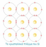 με τον πυρήνα, χωρίς να έχουν την ευκινησία των ηλεκτρονίων των αγωγών. Αν όμως, ένα ηλεκτρόνιο πάρει με κάποιον τρόπο πρόσθετη ενέργειας, τότε μπορεί να σπάσει τους δεσμούς του με τον πυρήνα και να φύγει απ΄ αυτόν. Η θέση από την οποία φεύγει το ηλεκτρόνιο είναι περιοχή με ηλεκτρονικό έλλειμμα, παρουσιάζει θετικό φορτίο ίσο με αυτό του ηλεκτρονίου και ονομάζεται οπή. Την πρόσθετη ενέργεια που πρέπει να πάρουν τα ηλεκτρόνια, για να φύγουν από το άτομο, μπορούμε να την προσφέρουμε με θερμότητα ή με φωτισμό. Το φως αποτελείται από μικρά σωματίδια, που λέγονται φωτόνια και τα οποία μεταφέρουν ενέργεια. Φωτίζοντας τον ημιαγωγό, κάποια από τα φωτόνια
 συγκρούονται με τα ηλεκτρόνια σθένους και μεταβιβάζουν σ΄ αυτά όλη τους την ενέργεια. Αν, λοιπόν, φωτίσουμε έναν κρύσταλλο Si, στο εσωτερικό του θα “δούμε” κάποια ηλεκτρόνια να εγκαταλείπουν τα αντίστοιχα άτομα και να προσκολλώνται σε άλλα. Στον κρύσταλλο θα υπάρχουν άτομα με 9 ηλεκτρόνια στην εξωτερική στοιβάδα, που θα είναι αρνητικά φορτισμένα, και άτομα με 7 ηλεκτρόνια στην εξωτερική στοιβάδα ή αλλιώς, με μια οπή στην εξωτερική στοιβάδα, που θα είναι θετικά φορτισμένα. Στο μεταξύ ελευθερώνονται κι άλλα ηλεκτρόνια που προσκολλώνται σε άτομα ή καταλαμβάνουν τη θέση μιας οπής που χάνεται. Αποτέλεσμα αυτής της διαδικασίας είναι μια άτακτη μετακίνηση ηλεκτρονίων και οπών, η οποία όμως δεν ισοδυναμεί με ηλεκτρικό ρεύμα. Το ηλεκτρικό ρεύμα είναι η κατευθυνόμενη και προς συγκεκριμένη φορά μετακίνηση ηλεκτρονίων ή οπών. Την κατευθυνόμενη κίνηση των ηλεκτρονίων και των οπών την πετυχαίνουμε με τους
 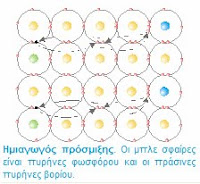 ημιαγωγούς πρόσμιξης. Ημιαγωγοί Πρόσμιξης : Ένας χημικά καθαρός ημιαγωγός δεν μπορεί να λειτουργήσει ως φωτοηλεκτρική γεννήτρια, εξαιτίας της άτακτης κίνησης των ηλεκτρονίων και των οπών στο κρυσταλλικό πλέγμα. Ας πάρουμε έναν κρύσταλλο Si και ας τον "νοθεύσουμε" με Φωσφόρο (Ρ) από τη δεξιά και με Βόριο (Β) από την αριστερή πλευρά του. Ο P και το B έχουν στην εξωτερική στοιβάδα αντίστοιχα 5 και 3 ηλεκτρόνια. Το ποσοστό της "νοθείας" ανέρχεται σε 1014 ως 1017 άτομα Ρ ή Β ανά cm3 κρυστάλλου Si. Με την πρόσμιξη στο κρυσταλλικό πλέγμα κάποια άτομα Si αντικαθίστανται από άτομα P και Β. Έτσι κάποια άτομα Si έχουν στη στοιβάδα σθένους 9 ηλεκτρόνια από την πλευρά που "νοθεύσαμε" με Ρ και 7 ηλεκτρόνια από την πλευρά που "νοθεύσαμε" με Β. Με άλλα λόγια, από την πλευρά του Ρ έχουμε πλεονάζοντα ηλεκτρόνια στις στοιβάδες σθένους, ενώ από την πλευρά του Β έχουμε ηλεκτρονικά ελλείμματα στις στοιβάδες σθένους, δηλαδή οπές. Όλος ο κρύσταλλος, όμως είναι ηλεκτρικά ουδέτερος. Αν φωτίσουμε το "νοθευμένο" κρύσταλλο, από την πλευρά του Ρ θα ελευθερωθούν ηλεκτρόνια (πλεονάζοντα), τα οποία, με άλματα θα κινηθούν προς την πλευρά του Β, για να καταλάβουν τα ηλεκτρονικά κενά, δηλ. τις οπές. Με αυτόν τον τρόπο θα διαπιστώσουμε στην περιοχή του Β συσσώρευση ηλεκτρονίων, δηλ. αρνητικών φορτίων και στην περιοχή του Ρ συσσώρευση οπών, δηλ. θετικών φορτίων. Έτσι πια μεταξύ των δύο "νοθευμένων" επιφανειών θα εκδηλωθεί ηλεκτρική τάση. Ο "νοθευμένος" κρύσταλλος του Si λειτουργεί ως ηλεκτρική πηγή με το θετικό πόλο από την πλευρά του Ρ και αρνητικό από την πλευρά του Β. Η σύνδεση των ακροδεκτών μιας λάμπας με τις δύο "νοθευμένες" περιοχές του κρυσταλλικού Si, θα συνοδεύεται από μετακίνηση ηλεκτρονίων, δηλ. από ηλεκτρικό ρεύμα.
~ Μητρόπουλος Αντώνης – μαθητής της Β' τάξης Λυκείου του Λεοντείου Λυκείου Νέας Σμύρνης.


| However the crystal is electric neutral. If light strikes the "doped" crystal, from the side of P will be released electrons (being redundant), which, with jumps will be moved to the side of B, in order to occupy the electronic voids, or the electron holes. In this way we will realise in the region of B accumulation of electrons, in other words negative charges and in the region of P accumulation of electron holes, or positive charges. So between the two surfaces of "doped" crystal electric tendency will be created. The "doped" crystal of Si functions as electric source with the positive pole from the side of P and negative pole from the side of B.Connecting a lamp to the two poles of "doped" crystal of Si, it will be accompanied by movement | Video from U.S. Department of Energy Photovoltaics Program |
of electrons, in other words from electric current.
~ Μitropoulos Αntonis – student of B' class of Lyceum of Lycée Léonin of Nea Smyrni.


No comments:
Post a Comment